This was originally not meant to be published - an internal "project".
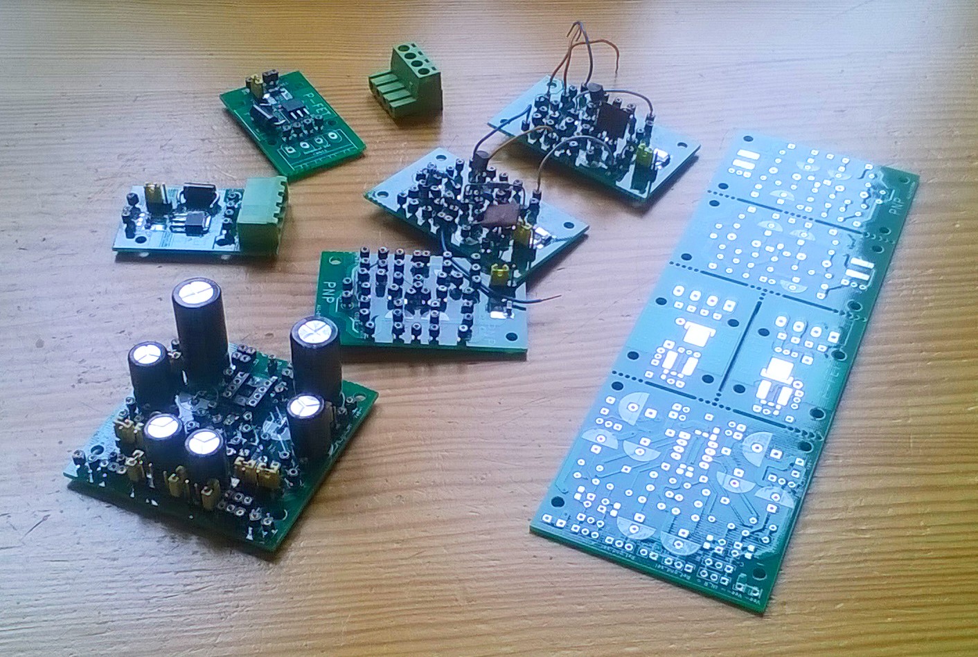
A set of universal boards for experiments with simple audio and basic transistor-based circuits.
Intended for cases where a breadboard is... too generic.
A breadboard doesn't have a ground plane, you cannot solder SMD's to it, it has contact resistances, various loop areas tend to be large, and you need to route *every* joint by wire bridges.
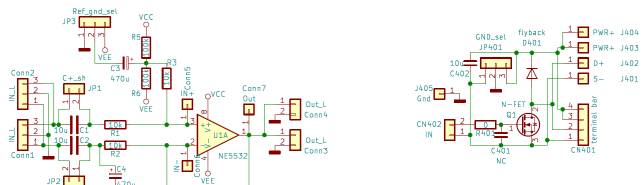
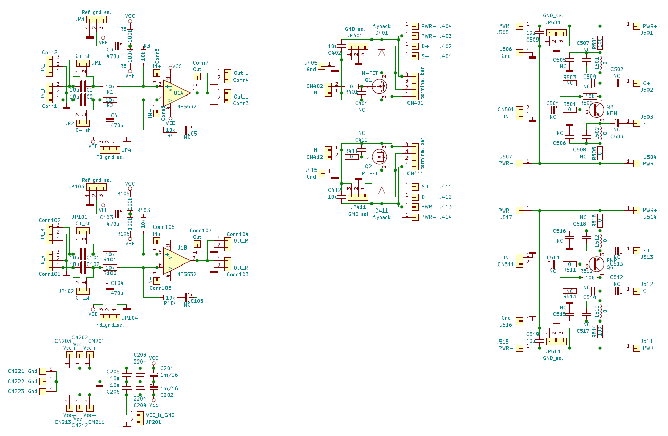
At the same time, the basic topology around an op-amp tends to be the same every time. Hell even the pinout of the parts tends to be standardized. So it makes sense, to throw a somewhat generic topology on a PCB. You can have all the traces properly routed for minimal loop area, have a solid GND layer under all of it, have power blocking/decoupling capacitors soldered where they belong.
Same thing with discrete transistors. Especially when you need a power switch,
the legs won't fit in a breadboard, and the best parts are nowadays SMD's,
while for the power path you'd use wiring terminals...
This again calls for a simple PCB with a somewhat universal topology.
Hence this "project".
The set of "tinker PCB's" presented here have have "too many components". This is for a purpose - feel free to adapt the schematic to the needs of a particular experiment, leaving footprints empty or putting a wire bridge where needed. Some positions are prepared for 2.5mm spaced pin headers, suitable for jumper caps - such as, to select your reference ground node in the op-amp circuit - thus accomodating a single supply or a split supply setup.
Schematic sheet in PDF
Kicad 4.0.7 project files (=source)
Gerbers for PCB manufacturing
You can solder THT resistors / capacitors straight into the holes, or you can solder "spring-loaded pin-holes", to have breadboard-like flexibility for particular positions. The pin-holes are sold in rows with 2.5 mm spacing, similar to pin headers... To interface to the PCB's, or to interconnect several of them, get some scraps of CAT5e or CAT6 cabling in the "solid wire" flavour (used for permanent installation in ducts).
The op-amp board is made for a dual op-amp in DIP8 package (suitable for socket mounting) in a stereo layout of the board. If you use an NE5532, it can work as a line output, but its output impedance is actually low enough to drive 32 Ohm headphones... i.e. no need for a dedicated headphone power stage.
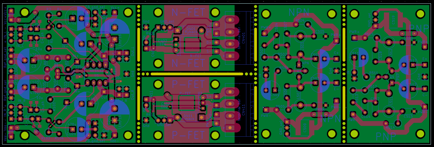
The transistors are labeled PNP/NPN and P-FET/N-FET, but the difference really is: you have two boards for the TO95 THT package, allowing for a wide variety of topologies, and two other boards for the TO251 power package, which looks like a crossover between a THT and SMD package (a brother of the SMD TO252 with THT legs).
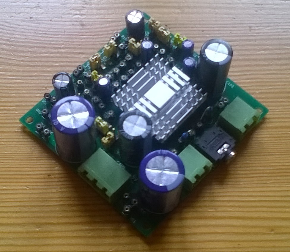
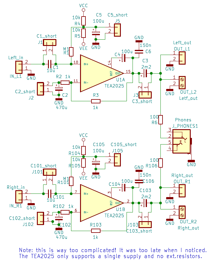
I also made a dedicated "power amp" board with the TEA2025. It can drive 8-ohm speakers, and the board also has a 3.5mm stereo jack for headphones. The resistors in series are there to attenuate the output level somewhat, for the headphones.
And I made the board much too complicated, because I didn't realize that you don't really have freedom in single- vs. split supply, and the inputs don't need (in fact, don't tolerate) DC biasing. This is done internally, on chip. I.e., no external resistors, period. I mean: with the TEA2025. Thus, most of the footprints on my existing board will forever remain empty :-) After I wired the board for single supply and skipped all the feedback and biasing resistors, the amp works just fine. See the "typical schematic" in the datasheet.
Schematic sheet in PDF
Kicad 4.0.7 project files (=source)
Gerbers for PCB manufacturing
Considering the broad availability of cheap and complete class-D power amp modules, I'm inclined to consider this a stillborn. No point building this, unless you specifically want a small class AB = linear amp, or a dedicated headphones amp. (And quite a noisy one at that. Well at least it's good old analog noise, not class D switch-mode EMI.)
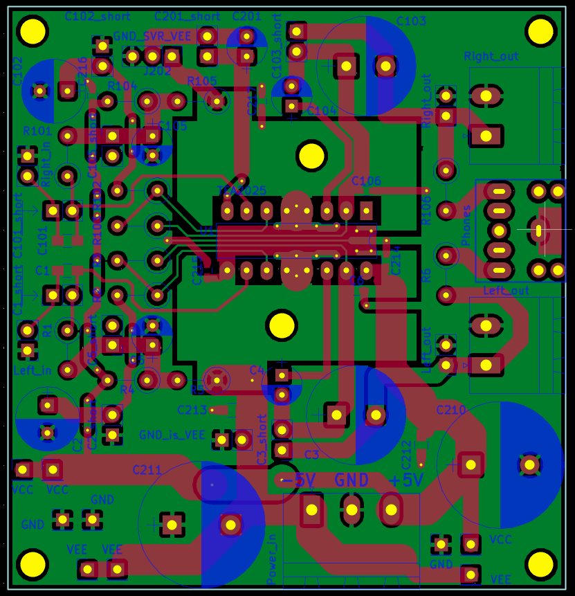
If you *do* venture to build this, consider paying attention to thermals. The TEA2025 is in a plastic DIP package, there is no heat transfer pad if memory serves. Except for the four DIP pins in the middle, see the board layout. Yet, there are ways to relieve the chip somewhat of the heat produced. Get some "thermocouple chewing gum", some variety that is electrically non-conductive. Or even just some non-conductive paste. The board has an area of bare copper on top, below the chip's belly, with extra vias going to the bottom side, which has more copper. This is your first heatsink. And, feel free to put another heatsink on top of the chip package, if you have some suitable lump of aluminum and enough skill to drill and maybe tap the two mounting holes.
Home | Contact | Česká verze